Lithography & Overlay
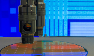
A semiconductor lithography system undertakes a process whereby highly complex circuit patterns drawn on a photomask made of a large glass plate are reduced using ultra-high-performance lenses and exposed onto a silicon substrate known as a wafer. Both the overlay of features to ensure proper layer to layer alignment, along with the actual photomask exposure, require specialized illumination techniques. DUV and EUV lithography have advanced technology to enable manufacturing of the smallest technology nodes possible.
However, new demands for more macro scale structures and devices to support heterogenous integration and BEOL advancements have opened the door to lower cost, higher power, more stable and longer lifetime illumination solutions.
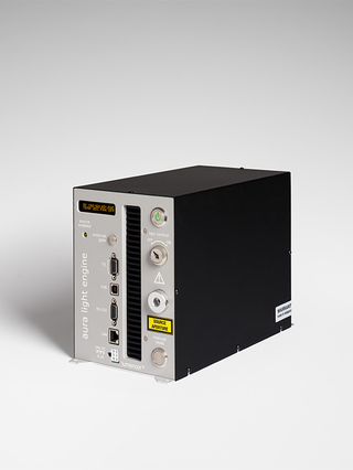
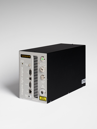
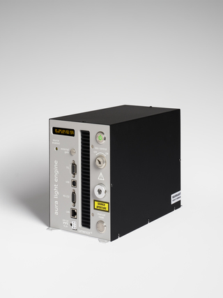
Commonly Used Products
Lithography & Overlay
Lithography & Overlay